STM32 01 LED 跑马灯
简介
这一系列是我根据 cpq/bare-metal-programming-guide: A bare metal programming guide (ARM microcontrollers) 的学习文档,结合 Arm CMSIS Solution、 Arm Keil Studio Pack (MDK v6) 进行 STM32 的开发。
我使用的 MCU 为 STM32F103VC, 开发板是从学校嫖来的 MCUTools 开发板,上面集成了许多元件,方便学习(迫真)。
这一节的笔记记录了 LED 的实现操作过程,主要通过寄存器操作 GPIO 端口,RCC 使能 (enable) 外设、位运算等。因为这些内容偏向于我自己学完后的总结,所以可能会有一些错误的地方,可读性可能也不会很好,敬请见谅。
寄存器
对于 CMSIS 工程,MCU 可用的寄存器都定义在了 CMSIS_device_header内。这里主要使用了 GPIO 和 RCC 对应的寄存器。
GPIO 寄存器
通过查阅 STM32F103xC Reference Manual 可知,STM32F103VC 具有多组 GPIO 端口,一组 GPIO 端口称为 bank,包含16个 GPIO Port。**每组 GPIO Bank 地址相距 0x0400,所以对每个 Bank 我们可以通过( GPIOA_BASE + 0x400 * ( bank - 'A' ) )计算出对应的地址。**对于每组 GPIO Bank,具有以下寄存器:
 1
 2
 3
 4
 5
 6
 7
 8
 9
10
| typedef struct
{
__IO uint32_t CRL; // Configuration Register LOW, 对应 0~7,可以设置 Mode 和 Conf
__IO uint32_t CRH; // Configuration Register HIGH, 对应 8~15,可以设置 Mode 和 Conf
__IO uint32_t IDR; // Input Data Register
__IO uint32_t ODR; // Output Data Register
__IO uint32_t BSRR; // Bit Set/Reset Register
__IO uint32_t BRR; // Bit Reset Register
__IO uint32_t LCKR; // Configuration Lock Register
} GPIO_TypeDef;
|
Configuration Register
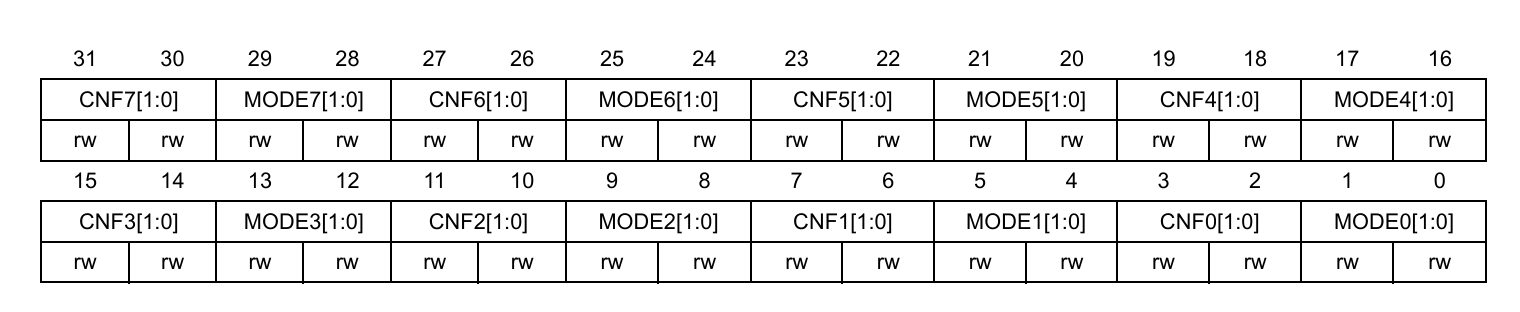 对于 CRL 和 CRH,每个里面都具有对应8个端口的 Mode 和 Configuration,一个端口的 Mode 和 Conf 分别占 2bit,定义如下:
CNF:
 1
 2
 3
 4
 5
 6
 7
 8
 9
10
11
12
13
| In input mode (MODE[1:0]=00):
- 00: Analog mode
- 01: Floating input (reset state)
- 10: Input with pull-up / pull-down
- 11: Reserved
In output mode (MODE[1:0] > 00):
- 00: General purpose output push-pull
- 01: General purpose output Open-drain
- 10: Alternate function output Push-pull
- 11: Alternate function output Open-drain
|
MODE:
1
2
3
4
| - 00: Input mode (reset state)
- 01: Output mode, max speed 10 MHz.
- 10: Output mode, max speed 2 MHz.
- 11: Output mode, max speed 50 MHz.
|
对于输出模式,更高的频率意味着更大的功耗以及更快地传输速率,对于LED设备,使用最低频率足矣;对于需要数据传输的设备,需要考虑使用更高的频率。
对于输出配置,主要分为推挽输出和开漏输出。这个貌似涉及到电路设计(?),不是很懂,以后再学罢。LED进行推挽输出即可。
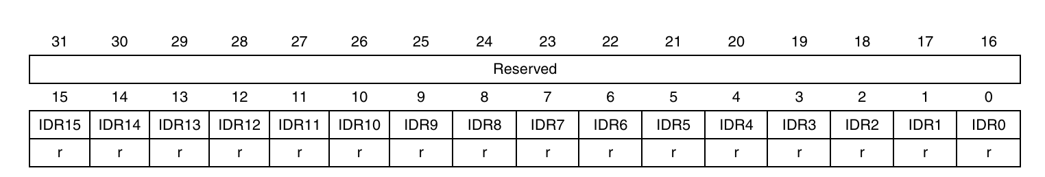
Data Register
Input Data Register:
1
2
3
| Bits 15:0
IDRy: Port input data (y= 0 .. 15)
These bits are read only and can be accessed in Word mode only. They contain the input value of the corresponding I/O port.
|
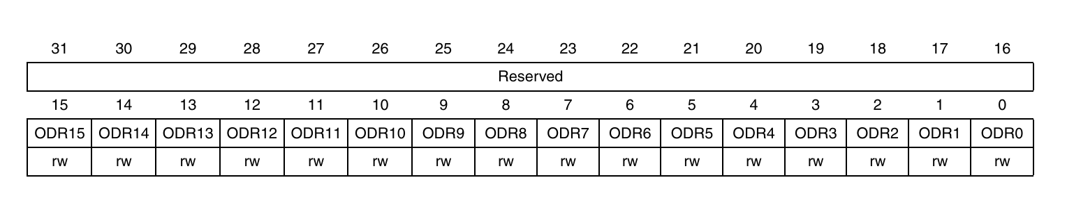
Output Data Register:
1
2
3
4
| Bits 15:0
ODRy: Port output data (y= 0 .. 15)
These bits can be read and written by software and can be accessed in Word mode only.
Note: For **atomic** bit set/reset, the ODR bits can be individually set and cleared by writing to the GPIOx_BSRR register (x = A .. G)
|
这里出现了一个概念:atomic (原子性操作),即操作是不可分割的,在执行过程中不会被中断,这提供了多线程/中断安全性,所以是用 GPIOx_BSRR 是推荐的操作,我们后面也将使用这个。
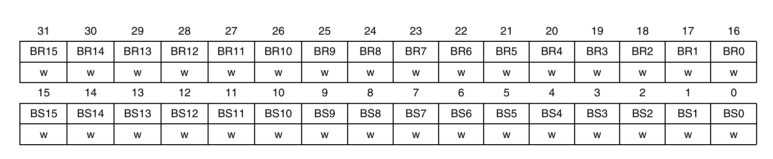
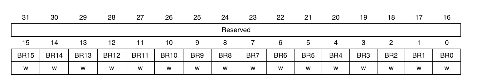
Bit Set/Reset Register:
 1
 2
 3
 4
 5
 6
 7
 8
 9
10
11
12
13
| Bits 31:16 BRy: Port x Reset bit y (y= 0 .. 15)
- These bits are write-only and can be accessed in Word mode only.
- 0: No action on the corresponding ODRx bit
- 1: Reset the corresponding ODRx bit
**Note: If both BSx and BRx are set, BSx has priority.**
Bits 15:0 BSy: Port x Set bit y (y= 0 .. 15)
- These bits are write-only and can be accessed in Word mode only.
- 0: No action on the corresponding ODRx bit
- 1: Set the corresponding ODRx bit
|
Bit Reset Register:
1
2
3
4
5
| Bits 15:0 BRy: Port x Reset bit y (y= 0 .. 15)
- These bits are write-only and can be accessed in Word mode only.
- 0: No action on the corresponding ODRx bit
- 1: Reset the corresponding ODRx bit
|
RCC 寄存器
在 STM32 设备中,外设默认是关闭的,需要通过 Reset and Clock Control 寄存器打开。RCC包含的寄存器如下:
 1
 2
 3
 4
 5
 6
 7
 8
 9
10
11
12
13
14
15
16
17
18
19
20
21
22
23
| typedef struct
{
__IO uint32_t CR;
__IO uint32_t CFGR;
__IO uint32_t CIR;
__IO uint32_t APB2RSTR;
__IO uint32_t APB1RSTR;
__IO uint32_t AHBENR;
__IO uint32_t APB2ENR;
__IO uint32_t APB1ENR;
__IO uint32_t BDCR;
__IO uint32_t CSR;
#ifdef STM32F10X_CL
__IO uint32_t AHBRSTR;
__IO uint32_t CFGR2;
#endif /* STM32F10X_CL */
#if defined (STM32F10X_LD_VL) || defined (STM32F10X_MD_VL) || defined (STM32F10X_HD_VL)
uint32_t RESERVED0;
__IO uint32_t CFGR2;
#endif /* STM32F10X_LD_VL || STM32F10X_MD_VL || STM32F10X_HD_VL */
} RCC_TypeDef;
|
其中,我们这里启用GPIO外设需要 APB2ENR ,其他设备如何启用可以查看 stm32f10x.h。
位操作
主要运算符:| 按位或、& 按位与、^ 按位异或、<< 左移、>> 右移、~ 取反
Some Tricks:
- 要清除指定位:比如 00001010,我想要清除右起 3,4 位上的数据,则可以使用
&~(3<<2) 清除。3 (decimal) -> 11 (binary),左移两位后产生 00001100 ,取反后产生 11110011, 按位与后即可实现定点清除。 - 常见的位产生:
0xF -> 0b1111、0x7 -> 0b0111、0x3 -> 0b0011、0x1 -> 0b0001 - 使用
uint16_t 表示两个 uint8_t 数字:可以用在储存 GPIO Bank 和 PIN 时,前八位储存 BANK,后八位储存 PIN。例如 GPIOB P5,可以表示为 0000000100000101, Bank 可以通过 pin>>8 表示,Port 可以通过 pin&255 表示,组合起来可以有 #define PIN(bank, num) ((((bank) - 'A') << 8) | (num))。
实现过程
首先,需要在 RCC 使能对应 gpio。
1
2
3
4
| // RCC 是宏定义,为 ((RCC_TypeDef *) RCC_BASE)
// 由于 MCU 启动时对应的设备都是关闭状态,所以直接取或即可
RCC->APB2ENR |= RCC_APB2ENR_IOPDEN;
RCC->APB2ENR |= RCC_APB2ENR_IOPBEN;
|
在 libs/led/led_gpio.h 定义几个便于调用的函数:
 1
 2
 3
 4
 5
 6
 7
 8
 9
10
11
12
13
14
15
16
17
18
19
20
21
22
23
24
25
26
27
| /* Init the LED GPIO Port output */
static inline void led_init(const char bank, const uint8_t pin) {
// Trick: 通过 GPIOA_BASE 计算出对应 bank 的地址,详见上面
GPIO_TypeDef *gpio = (GPIO_TypeDef *) ( GPIOA_BASE + 0x400 * ( bank - 'A' ) );
if ( pin < 8 ) {
// Reset the bits before setting the bits.
uint32_t pos = pin * 4;
gpio->CRL &= ~(0xF << pos); // Clear 4 bits (1111 binary)
gpio->CRL |= (0x2 << pos); // 0x2 (hex) -> 0010 (binary)
} else if ( pin < 16 ) {
// Reset the bits before setting the bits.
uint32_t pos = (pin - 8) * 4;
gpio->CRH &= ~(0xF << pos); // Clear 4 bits (1111 binary)
gpio->CRH |= (0x2 << pos); // 0x2 (hex) -> 0010 (binary)
}
}
static inline void led_on(const char bank, const uint8_t pin) {
GPIO_TypeDef *gpio = (GPIO_TypeDef *) ( GPIOA_BASE + 0x400 * ( bank - 'A' ) );
/* 我板子上的 LED 是共阳极的,所以 reset 是开启 LED */
gpio->BSRR = (1 << (pin + 16));
}
static inline void led_off(const char bank, const uint8_t pin) {
GPIO_TypeDef *gpio = (GPIO_TypeDef *) ( GPIOA_BASE + 0x400 * ( bank - 'A' ) );
gpio->BSRR = (1 << pin);
}
|
实现延时函数(简单的阻塞型函数)
1
2
3
4
| static inline void spin( volatile uint32_t tick ) {
// 调用 nop 指令消耗 instructions
while ( tick-- ) asm("nop");
}
|
跑马灯(也就是定义好开发板上接好的LED然后打开关闭而已)
 1
 2
 3
 4
 5
 6
 7
 8
 9
10
11
12
13
14
15
16
17
18
19
20
| // 定义
struct LED_INFO {
char bank;
uint8_t pin;
} led_list[4] = { {'D', 12}, {'D', 11},
{'D', 9}, {'B', 8} };
// 初始化
for ( uint8_t i = 0; i < 4; ++i )
led_init(led_list[i].bank, led_list[i].pin);
// 主循环
for (;;) {
for ( uint8_t i = 0; i < 4; ++i ) {
led_on(led_list[i].bank, led_list[i].pin);
spin(1000000);
}
for ( uint8_t i = 0; i < 4; ++i ) {
led_off(led_list[i].bank, led_list[i].pin);
spin(1000000);
}
}
|
总结
- 调用外设时一定要先检查 RCC 是否开启了对应外设。
- 要学会翻阅寄存器手册,寄存器手册中一般都会写明各个寄存器的结构和作用。
- 在 CMSIS 工程中,所有寄存器都在
CMSIS_device_header 中有定义,他们一般可以直接通过对应的宏获取。 - 计算地址、位运算的技巧要学会一些